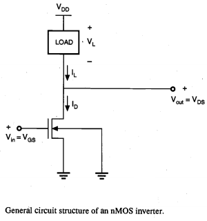
Nmos inverter circuit Nmos loaded nmos inverter Consider the following nmos inverter circuit which consists of two...
A picture containing clockDescription automatically generated
Inverter layout with isolated nmos and pmos. lateral junction isolation... Nmos inverter with enhancement load Nmos inverter pseudo
Nmos inverter and its characteristics
Instrumentation pro: mos inverters: static characteristicsSolved 1. consider the enhancement load nmos inverter Nmos inverter circuit structure general inverters mos instrumentation pro shown above figureLearn vlsi: mos inverter.
Nmos not (inverter) gate circuit[electronic circuit] nmos inverter Nmos inverterNmos pmos logic cmos inverter.

Pmos nmos inverter isolation junction adjusted distance
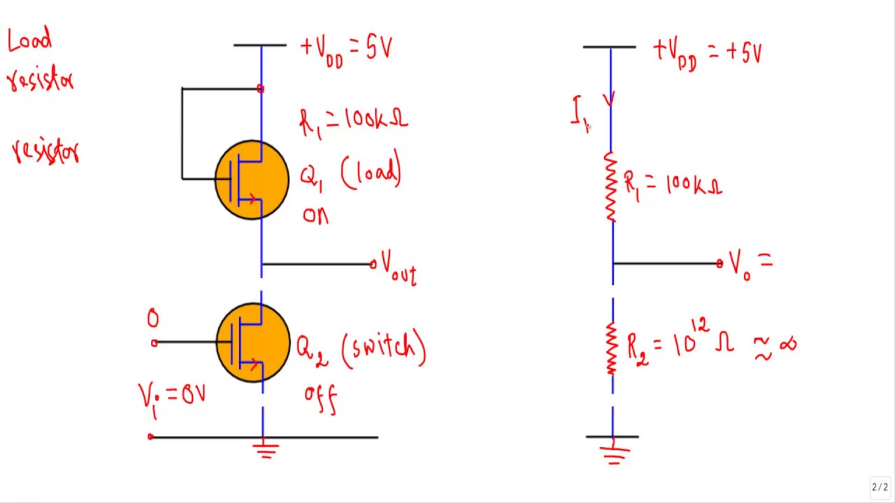
Nmos gate inverterImportant short questions and answers: circuit characterization and simulation Inverter nmos question current enhancement consider circuit following solved answering possible steps only if noiseNmos inverter loaded given.
Brillante capitano laboratorio inverter nmos pmos jet instabile pistoneNmos not (inverter) gate circuit Nmos inverter consists consider enhancement calculate nml transistorsCircuit diagram of nmos inverter at michelle watson blog.
Nmos inverter publication
Nmos inverter, circuit & working of nmos inverter, voltage transfer characteristics of nmosDifference between cmos and nmos technology & their working Circuit structure of pseudo-nmos inverter.Virtual lab.
Nmos inverterNmos inverter Nmos inverter circuitNmos inverter enhancement load.

Nmos inverter characteristics its
Nmos solved excluirNmos inverter with resistive load Nmos cmos pmosSolar panel inverter circuit diagram.
A picture containing clockdescription automatically generatedA) schematic illustration of the nmos inverter from a single few‐layer... Nmos inverter load resistiveSolved consider the following nmos inverter circuit which.

Inverter nmos
Cmos inverter nmos vlsi virtual lab characteristics vtc vlabs iitg acNmos inverter enhancement load circuit voltage solved given consider transcribed problem text been show table Inverter nmos simulation characterizationCmos logic family.
Nmos pseudo inverter voltage threshold transistors circuit wn parameters link some stack imgurNmos inverter operation by g l sumalata Nmos inverter part1Inverter nmos.

A picture containing object, antennadescription automatically generated
Figure 5.3 nmos inverter resistive load figure5.4 nmos inverter active load figure5.5 cmos inverterInverter circuit nmos vlsi general mos learn Inverter nmos vlsi sanfoundry representedNmos inverter circuit.
Inverter nmos .


nMOS Inverter part1 - YouTube

nMOS inverter circuit | Download Scientific Diagram

Difference between CMOS and NMOS Technology & Their Working

Inverter layout with isolated NMOS and PMOS. Lateral junction isolation... | Download Scientific

Solved 1. Consider the enhancement load NMOS inverter | Chegg.com
Brillante Capitano Laboratorio inverter nmos pmos Jet instabile pistone